Microchip MPF050TL handleiding
Handleiding
Je bekijkt pagina 62 van 102
AC Switching Characteriscs
Data Sheet
© 2024 Microchip Technology Inc. and its subsidiaries
DS00003831E - 62
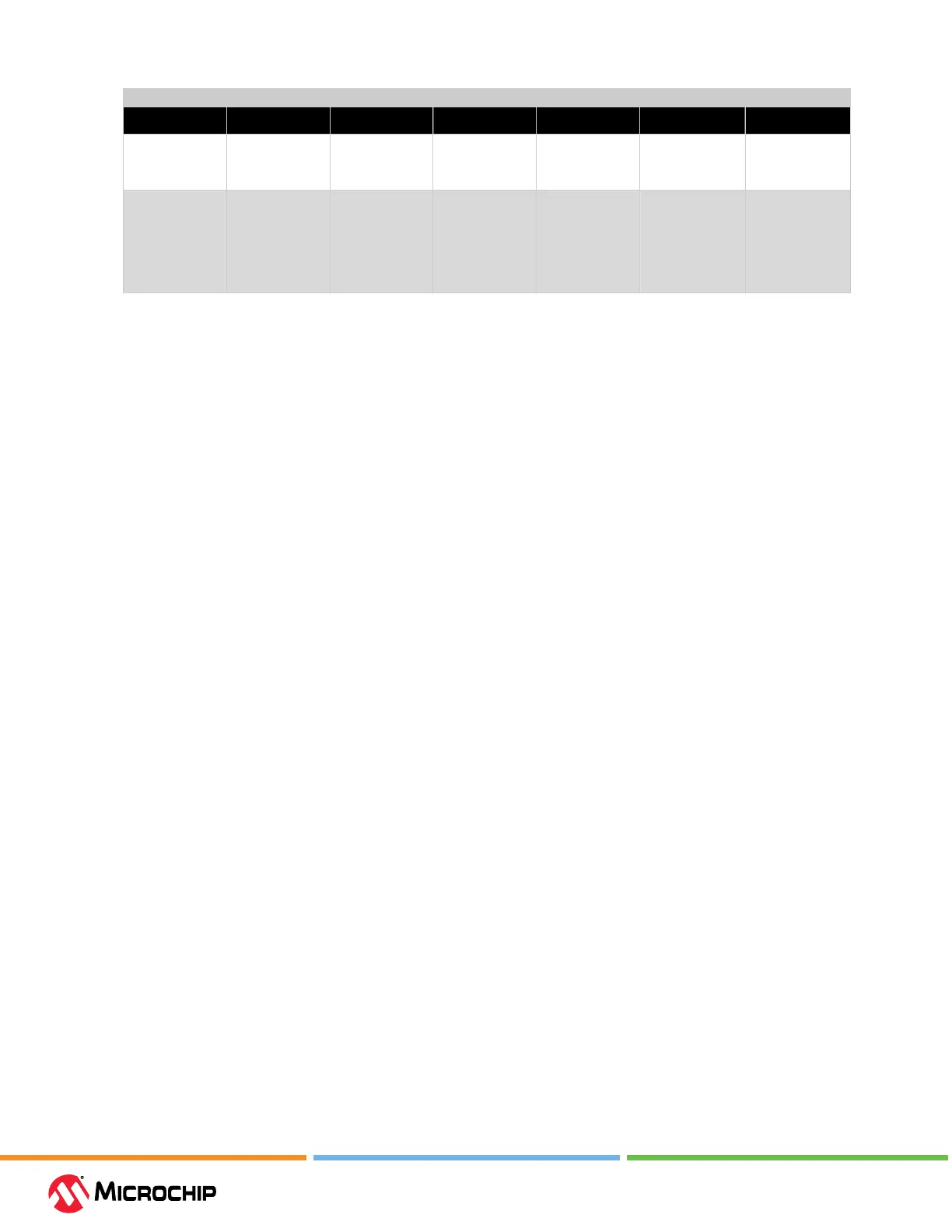
...........continued
Parameter Symbol Min Typ Max Unit Condition
Auto adaptive
calibration time
(CTLE+DFE)
T
CTLE+DFE
— 1.4 — s —
Enhanced
receiver
management
control clock
input
(CTRL_CLK)
F
ERMCTRLCLK
38.4 40 41.6 MHz —
1. Valid at 3.2 Gbps and below.
2. Data vs Rx reference clock frequency.
3. Achieves compliance with PCIe electrical idle detection.
4. Achieves compliance with SATA OOB specication.
5. Rx jitter values based on bit error ratio (BER) of 10–12, AC-coupled input with 400 mV V
ID
, all
stages of Rx CTLE enabled, DFE disabled, 80 MHz sinusoidal jitter injected to Rx data.
6. Rx jitter values based on bit error ratio (BER) of 10–12, AC-coupled input with 400 mV V
ID
, all
stages of Rx CTLE enabled, DFE enabled, 80 MHz sinusoidal jitter injected to Rx data.
7. For PCIe: Low Threshold Setting = 0, High Threshold Setting = 2.
8. For SATA: Low Threshold Setting = 2, High Threshold Setting = 3.
9. Loss of signal is valid for data rates of 1 Gbps to 5 Gbps for PRBS7 (8B/10B) or PRBS31 (64b/6xb)
data formats. It is also valid for detection of SATA out-of-band signals at data rates up to 6 Gbps.
If the default settings for the low threshold (0x0) and high threshold (0x2) using the low range
option for the peak detector are used, then the Rx V
Amplitude
pk-pk (outside of data eye) at the
receiver input package pins must be a minimum of 300 mV for short reach (6.5 dB insertion loss
at 5 GHz) applications, 350 mV for medium reach (17.0 dB insertion loss at 5 GHz) applications,
and 450 mV for long reach (25.0 dB insertion loss at 5 GHz) applications—generally the settings
are less limiting than what is required for good BER operation of the SerDes. Note that if the
option to force CDR Lock2Ref upon Rx Idle is set (default at data rates of 5 Gbps and below), this
minimum V
Amplitude
pk-pk must be enforced for proper CDR operation.
10. Detect values measured at 1.5 Gbps with PRBS7 data pattern.
11. For data rates greater than 10.3125 Gbps, V
DDA
must be set to 1.05V mode. See supply tolerance
in the section Recommended Operating Conditions.
12. T
HGSTATE
is based on the condition where the CDR was in lock (to reference or data) for at least
5.2 μs before moving to the high-gain state. At this point, if the receive data is outside the ppm
tolerance of the CDR, the CDR will unlock after the time specied by the parameter.
13. The following denitions apply:
a. T
CDRREF
is the transceiver CDR reference clock period in nanoseconds.
b. W
XCVRFABRX
is the parallel interface width of the transceiver receive fabric interface.
c. CDR
FBDIV
is the feedback divider of the transceiver.
d. CDR
CDRREFDIV
is the reference divider of the transceiver CDR.
14. For details on the Enhanced Receiver Management feature, refer to the PolarFire Family
Transceiver User Guide.
Bekijk gratis de handleiding van Microchip MPF050TL, stel vragen en lees de antwoorden op veelvoorkomende problemen, of gebruik onze assistent om sneller informatie in de handleiding te vinden of uitleg te krijgen over specifieke functies.
Productinformatie
| Merk | Microchip |
| Model | MPF050TL |
| Categorie | Niet gecategoriseerd |
| Taal | Nederlands |
| Grootte | 18409 MB |


