Microchip MPF050TL handleiding
Handleiding
Je bekijkt pagina 46 van 102
AC Switching Characteriscs
Data Sheet
© 2024 Microchip Technology Inc. and its subsidiaries
DS00003831E - 46
3. When cascading DLL into PLL, DLL output frequency should be limited such that the PLL
input jitter requirement is met. Refer to Table 5-18 and Table 5-19 for information on jitter
specications.
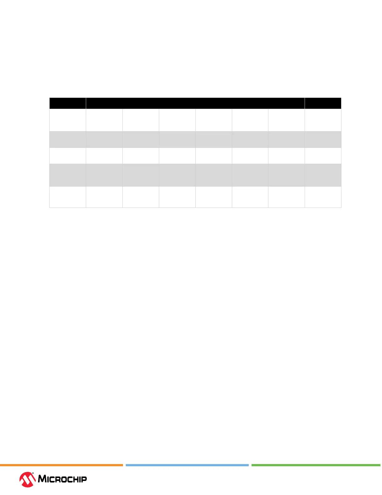
Table 5-24. Period Jier for External Output Clocks
6, 7, 8, 9
External output clocks are generated within the FPGA, routed through global networks and propagated outside of the
FPGA by means of HSIO or GPIO output buers. Jitter specications listed in this table are applicable to –STD and –1
speed grade for all temperature grades.
Parameter External Output Clock Period Jitter Unit
% FF used (of
total FFs in
device)
1,2
0% 14% 23% 47% 56% 75% %
Average
toggle rate
3
— 30% 30% 30% 30% 30% %
Eective FF
toggle %
4
0% 4.2% 6.9% 14.1% 16.8% 22.5% %
Max period
jitter
(absolute)
See Note 5 334 466 800 924 1140 ps
Max period
jitter (peak to
peak)
See Note 5 ±167 ±233 ±400 ±462 ±570 ps
1. % Flip-Flop (FF) used is dened as the percentage of total device FFs that are switching in the
largest clock domain within the FPGA (including synchronous and divided clocks).
2. The 50% and 75% FF used per clock domain are only shown to illustrate the impact of high
utilization on a global clock net jitter. Typical designs are expected to have less than 25% FF used
per clock domain (as dened in the preceding note).
3. Measured jitter is generated at varying % FF used levels with a switching rate of 30%.
4. Eective FF toggle % is the product of % FF used and average toggle rate. In Table 5-24, jitter is
specied for an average toggle rate of 30%. To determine jitter for a given combination, multiply
FF used and average toggle rate then use the linear interpolation equation as shown in Figure
5-5.
5. Use PLL, DLL, 160 MHz RC Osc jitter specications, or input jitter specications, as applicable.
6. All measurements were taken by observing the clock jitter from an FPGA output pin.
7. Refer to Table 5-25 for formulas to calculate period jitter as a function of the clocking topology.
8. For clock forwarded interfaces such as DDRx where both data and clock are sent from the same
clock domain, this external jitter component should be ignored. Output jitter should be taken
from the interface specication.
9. For further details, see the PolarFire Family Clocking Resources Users Guide (section Global Net
Clock Jitter).
Bekijk gratis de handleiding van Microchip MPF050TL, stel vragen en lees de antwoorden op veelvoorkomende problemen, of gebruik onze assistent om sneller informatie in de handleiding te vinden of uitleg te krijgen over specifieke functies.
Productinformatie
| Merk | Microchip |
| Model | MPF050TL |
| Categorie | Niet gecategoriseerd |
| Taal | Nederlands |
| Grootte | 18409 MB |


