Advantech IDK-2110P-1KXGA1 handleiding
Handleiding
Je bekijkt pagina 21 van 39
15 IDK-2110P-1KXGA1 User Manual
Chapter 2 LCD Display
2.7 Interface Timing
2.7.1 Input Signal Timing Specifications
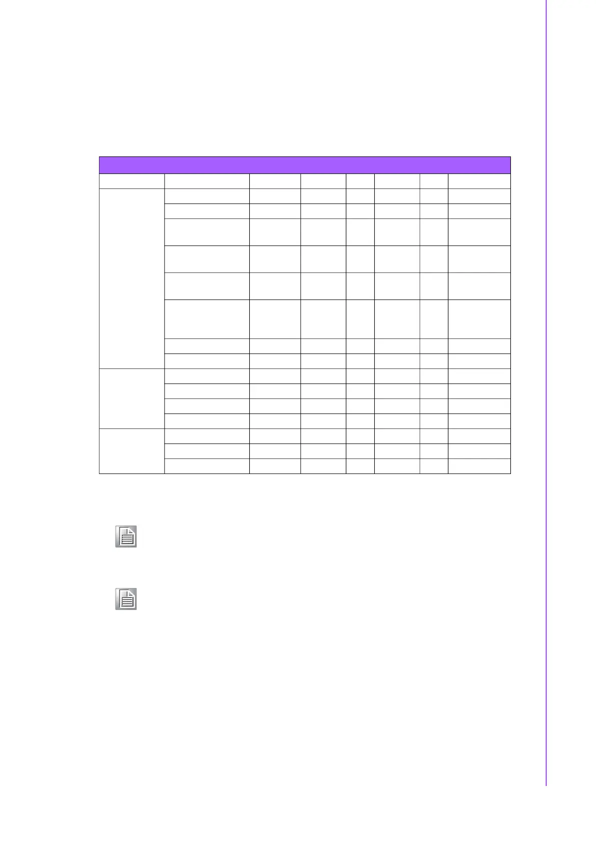
The input signal timing specifications are shown in the following table and timing dia-
gram.
Table 2.7: Display Timing Specifications
Signal Item Symbol Min. Typ. Max. Unit Note
LVDS Clock
Frequency Fc 57.7 65 73.6 MHz -
Period Tc 13.6 15.4 17.3 ns
Input cycle to
cycle jitter
Trcl --- --- 200 ns (a)
Input Clock to
data skew
TLVCCS -0.02*Tc --- 0.02*Tc ps (b)
Spread spectrum
modulation range
F
clkin_mod
0.987*Fc --- 1.013*Fc MHz (c)
Spread spectrum
modulation
frequency
FSSM --- --- 200 KHz
High Time Tch --- 4/7 --- Tch
Low Time Tcl --- 3/7 --- Tch
Vertical
Display
Term
Frame Rate Fr --- 60 --- Hz Tv=Tvd+Tvb
Total Tv 776 806 838 Th -
Active Display Tvd 768 768 768 Th -
Blank Tvb 8 38 70 Th -
Horizontal
Display
Term
Total Th 1240 1344 1464 Tc Th=Thd+Thb
Active Display Thd 1024 1024 1024 Tc -
Blank Thb 216 320 440 Tc -
Note (1) Because this module is operated by DE only mode, Hsync and Vsync
input signals should be set to low logic level or ground. Otherwise, this
module will operate abnormally.
Note (2) The Tv(Tvd+Tvb) must be integer; otherwise, the module will operate
abnormally.
Bekijk gratis de handleiding van Advantech IDK-2110P-1KXGA1, stel vragen en lees de antwoorden op veelvoorkomende problemen, of gebruik onze assistent om sneller informatie in de handleiding te vinden of uitleg te krijgen over specifieke functies.
Productinformatie
| Merk | Advantech |
| Model | IDK-2110P-1KXGA1 |
| Categorie | Niet gecategoriseerd |
| Taal | Nederlands |
| Grootte | 4433 MB |


