Handleiding
Je bekijkt pagina 18 van 39
IDK-1115P User Manual 12
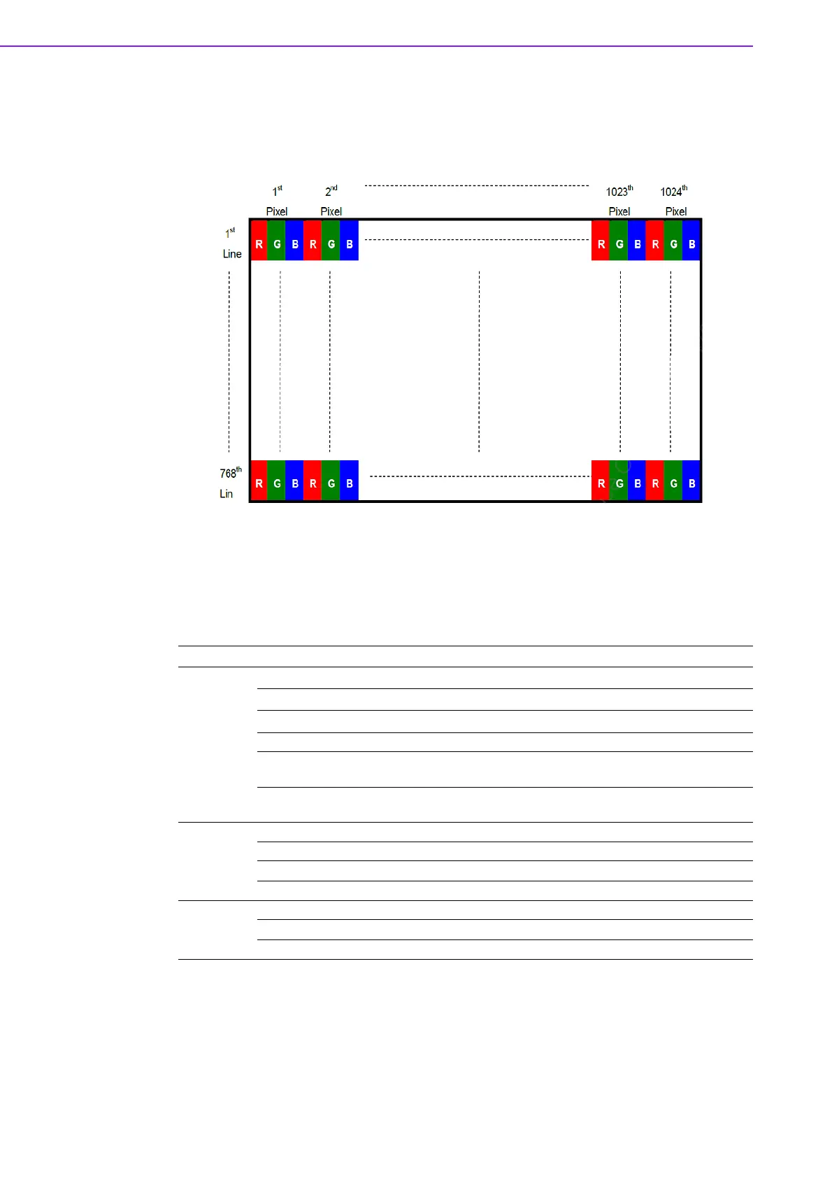
3.1 Pixel Format Image
The following figure shows the relationship between the input signal and the
LCD pixel format.
3.2 Input Signal Timing Specifications
The input signal timing specifications are shown as the following table and timing dia-
gram.
Note 1: Because this module is operated by DE only mode, Hsync and Vsync input
signals should be set to low logic level or ground. Otherwise, this module
would operate abnormally.
Note 2: The Tv (Tvd+Tvb) value must be an integer, otherwise, the module will oper-
ate abnormally.
Signal Item Symbol Min. Typ. Max. Unit Note
LVDS Clock
Frequency F
c
53.35 65 80 [MHz] -
Period T
c
12.5 15.38 18.75 [ns]
Input cycle to cycle jitter T
rcl
--- --- 200 [ns] (a)
Input Clock to data skew TLVCCS -0.02*Tc - 0.02*Tc [ps] (b)
Spread spectrum
modulation range
F
clkin_mod
- - 1.02*Fc [MHz] (c)
Spread spectrum
modulation frequency
F
SSM
--200[KHz]
Vertical
Display
Term
Frame Rate Fr 55 60 70 [Hz] Tv=Tvd+Tvb
Total Tv 780 806 840 [Th] -
Active Display Tvd 768 768 768 [Th] -
Blank Tvb Tv-Tvd 38 Tv-Tvd [Th] -
Horizontal
Display
Term
Total Th 1240 1344 1360 [Tc] Th=Thd+Thb
Active Display Thd 1024 1024 1024 [Tc]
Blank Thb Th-Thd 320 Th-Thd [Tc]
Bekijk gratis de handleiding van Advantech IDK-1115, stel vragen en lees de antwoorden op veelvoorkomende problemen, of gebruik onze assistent om sneller informatie in de handleiding te vinden of uitleg te krijgen over specifieke functies.
Productinformatie
| Merk | Advantech |
| Model | IDK-1115 |
| Categorie | Monitor |
| Taal | Nederlands |
| Grootte | 3607 MB |


